


Environmental Test Chambers for JESD22-A105C Power and Temperature Cycling
This test method applies to semiconductor devices that are subjected to temperature excursions and required to power on and off during all temperatures. And for sure, you certainly need a environmental test chamber to reach those specific temperatures.
The power and temperature cycling test is performed to determine the ability of a device to withstand alternate exposures at high and low temperature extremes with operating biases periodically applied and removed. It is intended to simulate worst case conditions encountered in typical applications. The power and temperature cycling test is considered destructive. It is intended for device qualification.
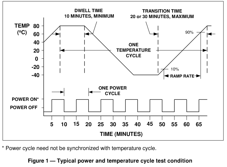
Temperature cycle time is the time between one high temperature extreme to the next, or from one low temperature extreme to the next.
Ramp rate is the rate of temperature increase or decrease per unit of time for the samples. Ramp rate should be measured for the linear portion of the profile curve, which is generally the range between 10% and 90% of the test condition temperature range .
Dwell time is the amount of time the sample temperature that has exceeded the specific temperature, either the high or the low temperature.
Power cycle time is the time between one power on to the next, or from one power off to the next.
The apparatus required for this test shall consist of a controlled temperature chamber capable of producing the specified temperatures within the specified transition times.

Sockets or other mounting means shall be provided within the chamber so that reliable electrical contact can be made to the device terminals in the specified circuit configuration. Power supplies and biasing networks shall be capable of maintaining the specified operating conditions throughout testing period despite normal variations in line voltages or ambient temperatures.
The test circuity should also be designed so that existence of abnormal or failed devices does not alter the specified conditions for other units on test. Care should be taken to avoid possible damage from transient voltage spikes or other conditions that might result in electrical, thermal, or mechanical over-stress.
When special mounting or heat sinking is required, the details shall be specified in the applicable specification. The power should then be applied and suitable checks made to assure that all devices are properly biased. During the test, the power applied to the devices shall be alternately cycled 5 minutes on 5 minutes off unless otherwise specified in the applicable specification.
The devices shall concurrently be cycled between temperature extremes for the specified number of cycles. The time at the high and low temperature extremes shall be sufficient to allow the total mass of each device under test to reach the specified temperature extremes with no power applied. The low temperatures to high temperature transition or reverse sequence is acceptable.
The power and temperature cycling test shall be continuous except then parts are removed from the chamber for interim electrical measurements. If the test is interrupted as a result of power or equipment failure, the test may restart from the point of stoppage.
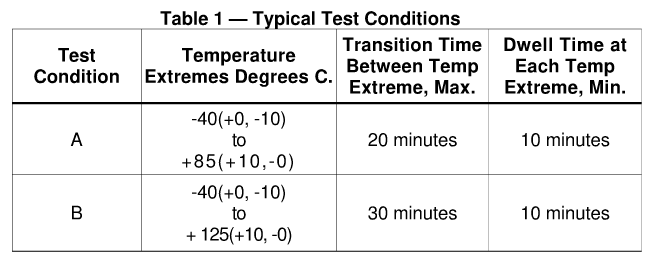
The electrical bias circuit shall be specified in the applicable specification. The device shall be subjected to the test conditions derived from Table 1 as illustrated in Figure 1.
If liquid nitrogen is used, care must be taken to avoid direct exposure of the parts and boards to the liquid nitrogen. The yest setup should be monitored initially and at the conclusion of a test interval to establish that all devices are being stressed to the specified requirements. Deviations must be corrected prior to further cycling to assure the validity of the qualification data.
Devices with solder interconnects have cycle rates that are in the range of ˂ 1 to 2cph. These include flip chip, ball grid array and stacked packages with solder interconnections. Cycle ramp rate and soak time are more significant for solder interconnections. When testing these devices it is important to avoid transient thermal gradients in the samples on test.
Samples with large thermal mass and low heat transfer efficiency require ramp rates slow enough to compensate for the thermal mass. The temperature of the sample should be within a few degrees of the ambient temperature during the temperature ramps. Typical ramp rate for this situation is 15℃/min or less for any portion of the cycle. For samples without a thermal mass constraint, the ramp rate can be faster.
The procedure of test A from Table 1 is as below:
Temperature range: -40℃~ 85℃ 6.25℃min≤ Temp rate ≤ 15℃/min
Sample power cycling: 5min on and 5min off
When chamber’s temperature reaches 85℃, hold it for 10min.
Temperature from 85℃ to -40℃ must within 20min.
When chamber’s temperature reaches -40℃, hold it for 10min.
Temperature from -40℃ to 85℃ must within 20min.
This is a whole loop which needs 60min.
According to the temp rate, you can see how fast the temperature changes. If you wanna reach those extreme temperature, a climatic test chamber is necessary.
For more details, please feel free to contact sales@lenpure.com.
Please visit www.lenpure.com


